Table of Contents
1. Introduction & Overview
This document presents a comprehensive numerical simulation and analysis of a novel GaN-based bipolar cascade laser (BCL) design. The laser features a unique architecture with multiple active regions separated by tunnel junctions (TJs) and employs surprisingly wide InGaN quantum wells (QWs). The primary goal is to understand the internal device physics, identify performance bottlenecks, and explore design optimization strategies to overcome efficiency limitations that have hindered the realization of high-performance cascaded GaN lasers using traditional metal-organic vapor-phase epitaxy (MOVPE).
2. Device Structure & Design
The analyzed device is a blue-emitting laser diode fabricated using plasma-assisted molecular beam epitaxy (PAMBE). Its core innovation lies in the vertical stacking of two single-quantum-well active regions, interconnected by a heavily doped InGaN tunnel junction for carrier recycling.
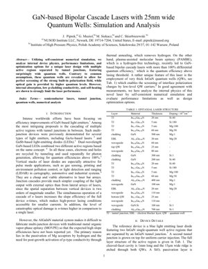
2.1 Epitaxial Layer Structure
The detailed layer structure is summarized in the table below, highlighting key components like the tunnel junctions (TJ), electron blocking layer (EBL), waveguides, and the active quantum wells.
- Cavity Length: 1 mm
- Ridge Width: 15 μm
- Top QW Composition: In0.18Ga0.82N, 25 nm
- Bottom QW Composition: In0.17Ga0.83N, 25 nm
- Tunnel Junction: Heavily doped n++/p++ InGaN layers
2.2 The Role of Wide Quantum Wells
Contrary to conventional laser designs using thin QWs (~3 nm), this device employs exceptionally wide QWs (25 nm). This design choice is critical for mitigating the strong piezoelectric and spontaneous polarization fields inherent to nitride heterostructures, which typically cause quantum-confined Stark effects (QCSE) that reduce radiative efficiency.
2.3 Tunnel Junction Design
The tunnel junction is a pivotal element, enabling the series connection of the two active regions. It allows electrons from the n-side of one junction to tunnel into the p-side of the next, effectively "recycling" carriers and aiming for differential quantum efficiencies exceeding 100% above threshold.
3. Core Physics & Simulation Insights
Self-consistent numerical simulations (likely employing drift-diffusion and quantum mechanical models) reveal the intricate internal physics governing this device.
3.1 Polarization Field Screening
A key finding is that the wide QWs enable near-perfect screening of the built-in polarization field by carriers injected at relatively low densities. The screening charge density $\rho_{screen}$ required can be approximated by relating it to the polarization discontinuity $\Delta P$ at the interfaces: $\rho_{screen} \approx - \Delta P / q d_{QW}$, where $q$ is the elementary charge and $d_{QW}$ is the well width. The large $d_{QW}$ reduces the required carrier density for effective screening.
3.2 Gain Mechanism from Higher Levels
Due to the wide well, the electron and hole wavefunctions are more spatially separated in the fundamental sub-bands, reducing their overlap and thus the optical matrix element. Surprisingly, the simulations indicate that significant optical gain is instead provided by transitions involving higher quantum confined energy levels (e.g., e2-hh2), where the wavefunction overlap is restored.
3.3 Performance Limiting Factors
The analysis identifies three major bottlenecks:
- Internal Absorption: Significant optical loss within the p-type cladding and contact layers.
- Low p-Cladding Conductivity: High series resistance leading to excessive Joule heating.
- Self-Heating: The combined effects of series resistance and non-radiative recombination elevate the active region temperature, reducing gain and efficiency.
4. Results & Performance Analysis
The simulation results are validated against experimental data from the fabricated device.
4.1 Simulated vs. Measured Characteristics
Good agreement is found between simulated and measured light-current (L-I) and voltage-current (V-I) characteristics, particularly in pulsed operation. The model successfully reproduces the threshold current and the slope efficiency, confirming the accuracy of the identified physical mechanisms.
(Note: Based on described physics, a conceptual chart would show) A band diagram across the two active regions and the central tunnel junction under forward bias. Key features would include:
- Flattened bands within the wide QWs due to polarization field screening.
- High carrier densities in the QWs sufficient for screening and gain.
- The alignment of bands in the heavily doped TJ region, enabling interband tunneling.
- Voltage drops highlighting the high resistance in the p-type cladding layers.
4.2 Key Performance Metrics
The device demonstrates the principle of carrier recycling, with a differential quantum efficiency above 100% in pulsed mode, as reported in the referenced experimental work. However, the simulated analysis clearly shows that the identified limitations (absorption, resistance, heating) severely cap the performance in CW mode, preventing the full potential of the cascade concept from being realized.
5. Optimization Pathways & Future Directions
Based on the simulation insights, several concrete optimization routes are proposed:
- Cladding Layer Engineering: Replacing or modifying the p-type AlGaN cladding with lower-resistance alternatives, such as graded layers or the use of polarization-doped layers, to reduce series resistance and associated heating.
- Optical Mode Management: Redesigning the waveguide to better confine the optical mode away from lossy p-type contact layers, reducing internal absorption.
- Advanced TJ Design: Exploring alternative TJ materials or doping profiles to lower the voltage drop across the junction itself.
- Thermal Management: Implementing more effective heat sinking strategies or substrate removal techniques to mitigate self-heating effects.
- Integration with MOVPE: The success of PAMBE-grown devices highlights a path forward. Future work may focus on developing hydrogen-free doping schemes or low-temperature activation processes compatible with mainstream MOVPE to enable scalable production of high-efficiency cascade lasers.
6. Analyst's Perspective: Core Insight & Critique
Core Insight: This work brilliantly demonstrates a "physics-first" workaround to a materials science dead-end. The GaN community has long struggled with inefficient p-type doping and polarization fields. Instead of waiting for a miraculous new doping technique, the authors use a wide QW to neuter the polarization problem and a tunnel junction to bypass the need for efficient hole injection across multiple stages. It's a clever, simulation-guided hack that gets to the core function—carrier recycling—by sidestepping traditional limitations.
Logical Flow: The argument is compelling: 1) Wide QWs screen polarization, flattening bands. 2) Flatter bands allow higher-level transitions to provide gain. 3) Tunnel junctions recycle carriers for multi-stage efficiency. 4) However, legacy issues (p-type resistance, absorption) inherited from standard laser design now become the dominant bottlenecks. The simulation elegantly traces the performance ceiling back to these well-known, yet unsolved, secondary problems.
Strengths & Flaws: The strength is undeniable—theoretical prediction and experimental validation of >100% quantum efficiency is a landmark. The use of PAMBE to avoid hydrogen passivation is a key enabler, as noted in reports from institutions like the University of California, Santa Barbara, which highlight hydrogen's role as a major acceptor compensator in MOVPE-grown GaN. The flaw, which the authors openly address, is that the solution is incomplete. It solves the primary quantum efficiency problem but amplifies thermal and resistive issues. It's like building a high-performance engine but connecting it with a corroded fuel line.
Actionable Insights: For researchers, the message is clear: the next breakthrough won't be in the active region design—that's largely solved here—but in the cladding and contact engineering. Focus must shift to developing low-resistance, low-absorption p-type layers, perhaps using novel concepts like polarization-induced doping or metastable alloys. For industry, this paper signals that PAMBE, not MOVPE, might be the near-term pilot line technology for advanced cascade devices, potentially reshaping investment in epitaxy tools. The work serves as a detailed blueprint, identifying exactly which knobs to turn next.
7. Technical Appendix
7.1 Mathematical Framework
The simulation likely employs a system of coupled equations:
- Poisson's Equation: $\nabla \cdot (\epsilon \nabla \psi) = -\rho(\psi, n, p)$ to solve for the electrostatic potential $\psi$, accounting for doping, mobile carriers (n, p), and fixed polarization charges.
- Drift-Diffusion Equations: $\vec{J}_n = q \mu_n n \vec{E} + q D_n \nabla n$ and $\vec{J}_p = q \mu_p p \vec{E} - q D_p \nabla p$ for carrier transport, with appropriate models for recombination (Shockley-Read-Hall, Auger, radiative).
- Quantum Mechanical Solver: A Schrödinger equation solver (e.g., using the effective mass approximation) within the QW regions to determine confined energy levels $E_i$ and wavefunctions $\xi_i(z)$: $[-\frac{\hbar^2}{2} \frac{d}{dz}\frac{1}{m^*(z)} \frac{d}{dz} + V(z)]\xi_i(z) = E_i \xi_i(z)$.
- Optical Gain Calculation: The material gain $g(\hbar\omega)$ is computed from the interband transition matrix elements and Fermi-Dirac distributions for carriers in the quantized sub-bands.
7.2 Analysis Framework Example
Case Study: Parameter Sweep for p-Cladding Conductivity
Objective: Quantify the impact of improving p-cladding conductivity on CW output power.
Method: Using the calibrated simulation model, systematically vary the hole mobility $\mu_p$ or the effective doping concentration $N_A$ in the p-AlGaN cladding layers. For each value, perform a self-consistent CW simulation at a fixed current above threshold.
Metrics to Track:
- Junction temperature rise ($\Delta T$).
- Voltage drop across the cladding layers.
- Change in modal gain due to temperature-induced bandgap shrinkage.
- Net change in optical output power.
8. References
- Nakamura, S., et al. "The Blue Laser Diode: The Complete Story." Springer, 2000. (Seminal work on GaN light emitters).
- Ryou, J.-H., et al. "Control of quantum-confined Stark effect in InGaN-based quantum wells." IEEE J. Sel. Top. Quantum Electron., 2009. (Discusses polarization field management).
- Simon, J., et al. "Polarization-induced Zener tunnel junctions in wide-band-gap heterostructures." Phys. Rev. Lett., 2009. (Background on nitride tunnel junctions).
- Muziol, G., et al. "GaN-based bipolar cascade laser with 106% differential quantum efficiency in pulsed mode." Appl. Phys. Express, 2019. (The primary experimental work analyzed in this PDF).
- Piprek, J. "Semiconductor Optoelectronic Devices: Introduction to Physics and Simulation." Academic Press, 2003. (Source for numerical simulation methodologies).
- U.S. Department of Energy. "Solid-State Lighting R&D Plan." 2022. (Highlights efficiency goals and challenges for next-generation light sources, relevant to the pursuit of >100% quantum efficiency devices).